Synopsys Cloud
Cloud native EDA tools & pre-optimized hardware platforms
Request a Free Trial →
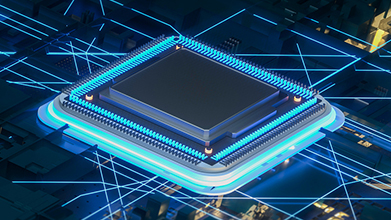
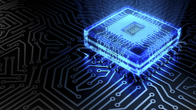
As Moore’s law slows, engineering ingenuity has created innovative ways to push the boundaries of physics. Multi-die chip designs, whose heterogeneous integration of semiconductor dies enable better bandwidth, performance, and yield, have emerged from this. In addition to packaging advancements, what has also made multi-die chip designs possible is the Universal Chiplet Interconnect Express (UCIe) standard for die-to-die connectivity.
By mixing and matching dies, or chiplets, from different vendors and even foundry process nodes, chip designers gain the flexibility to target particular dies to particular functions. Not all functions need to be on the most advanced nodes, so designers can potentially capture some cost savings while attaining an easier way to adapt their chip designs for different product variants. UCIe IP standardizes die-to-die connectivity and enables disparate dies to talk to each other.
What’s more, sourcing IP from a single vendor allows you to take advantage of a complete chip design and verification flow with IP for a variety of process technologies (even if the dies in your design come from multiple vendors and foundry process nodes). Other benefits of this approach include:
Synopsys, which provides a broad UCIe IP solution optimized for the major foundries and for standard and advanced packaging, has witnessed how these benefits can be realized across the major foundries. Read on to learn more about the gains of mixing and matching dies in a single package and how UCIe IP from a single vendor supporting multiple foundries and multiple nodes can lead you to silicon success.

As adoption of multi-die chip designs continues to grow, particularly for bandwidth-hungry applications, UCIe provides assurance. Despite increasing popularity, there’s still a fair amount of anxiety about multi-die architectures because, in the scheme of things, they are relatively novel. Compared to other emerging die-to-die specifications, UCIe defines a complete stack for the die-to-die interconnect. As such, UCIe provides the assurance of interoperability and seamless connectivity. In addition, as more dies are integrated into a single package, this creates greater latency. UCIe IP can help maintain latency while reducing power and enhancing performance. With redundant lanes between the two sides of the PHY, the UCIe specification ensures high reliability and enables repairs through these extra lanes.
Once designers become accustomed to a vendor’s IP, being able to stay with that vendor for other IP solutions enables them to maintain consistency in the methodologies and flows they’ve set up. Having a similar set of IP-related deliverables across different nodes can also accelerate the design implementation and verification processes.
Synopsys understands the unique challenges of multi-die designs and intends to make the journey easier. Synopsys UCIe IP, which includes the controller, PHY, and verification IP, has achieved silicon success on numerous foundry process nodes, and we’re collaborating with our foundry partners to develop UCIe IP for several more process nodes, giving designers flexibility to realize the advantages of mixing and matching heterogeneous dies in a single package.
Since it was released in 2022, the UCIe standard has continued to evolve as adoption grows. While it has primarily been a die-to-die communication specification, there’s potential for UCIe to eventually become more of a chiplet specification that defines compliance for the die-to-die interface, guides how chiplets are managed and controlled, and outlines security for chiplets and multi-die designs.
As a member of the UCIe Consortium, Synopsys collaborates with other industry leaders to help shape the evolution of the standard. Through our expertise in IP development as well as multi-die designs, we can help take multi-die concepts to the finish line. With multi-die designs breathing new life into Moore’s law, UCIe looks to play a key role in influencing the future of the semiconductor industry.
Mar 15, 2024 / 8 min read